COMPACT is the Interreg Nord, European Regional Development Fund (ERDF) project that works from the premise that an honest research can generate new job opportunities. It is well known that up-north of Sweden and Finland are always remained in isolation mainly due to low population density and cold-weather influenced living environment. Most important this area has low economic growth compared to the southern part of the countries. Thus, it becomes essential in this region to induce the growth through collaboration like development of new competence for the regional business community. High Density Interconnects (HDI) PCBs manufacturing market is expected to grow from USD 9.5 billion in 2018 to USD 16.9 billion by 2023, at a CAGR of 12.3% from 2018 to 2023. Thus, it can be seen that HDI-PCBs soon be applied to nearly every electronics gadget that is under the use. Presently, few major players from EU, USA and China has this capability to manufacture HDI-PCBs.
The project COMPACT is an attempt to bring-up a high desity PCB manufacturing methodology to SMEs present in the northern region to compete with the well established industries in the field. COMPACT tends to set a platform for economical upgrading of the SMEs using the research conducted by the domain experts of the northern universities of both Sweden and Finland.
The project constitutes of three stages. First, design and development of interconnects using the SBU technology based on Covalent Bonding Metallization (CBM). The next stage is to perform the reliability analysis of developed structures. Finally, standardization of the process for commercial purposes using the design and analysis data.Thus, this research, design, fabricates and evaluates methods and tools will support the northern SME in creating their presence on globe in HDI- manufacturing facilities
The focus of this work is to develop a cost-efficient, flexible and reliable fabrication methodology that will be suitable for bulk production pf PCBs. The work is planned to be done using Sequential Build Up (SBU) process where the methodology used is fully additive and feasible at room temperature.
Few of the outcomes of the project would be greatly miniaturized electronics devices with new manufacturing technology, Reduced manufacturing time and costs with completive products , Improved and managed reliable devices for customers, More environmental friendly manufacturing due to the lower amount of chemicals and easier waste management , Growth of the regional industry according to Industry 4.0 norms, New scientific results and practical outcomes for all partners and general audience and many more.
The EU program Interreg Nord supports cross-border cooperation with the intention of strengthening economic and social development during the period 2014-2020. The overall goal of the Nordprogramme is to strengthen the program area's competitiveness and attractiveness. The program includes northern Sweden, northern Finland, northern Norway and Sápmi. The region differs from other European areas by its Arctic features with cold climates, polar nights, large natural areas and abundant natural resources.

The overall goal of Interreg Nord 2014-2020 is to strengthen the competitiveness and attractiveness of the programme area. To achieve the overall goal, the region’s development needs to take place in an economically, socially and environmentally sustainable manner. This is achieving this through funding the cross-border cooperation that will address the common challenges identified in the border regions and make use of under-utilised opportunities in the border areas. At the same time, the collaborative process needs to be strengthened which will generally foster harmonious development within the EU and its neighboring countries. Thus, the Interreg Nord is working continuously in building common conditions for the northern region of Sweden, Finland and Norway to further develop a resource-efficient, environmentally friendly, competitive and low-carbon society

The Regional Council of Lapland is a statutory joint municipal authority, the members of which are all of the 21 municipalities of Lapland. The council’s work centres on the wellbeing of Lapland’s people, as well as the living force, pulling force and holding force of Lapland. This is achieving via the vision of “We are an inspired, “consider it done” team that gives a positive boost to Lapland. We promote the success of Lapland and the wellbeing of the people of Lapland”. The core tasks of the Regional Council of Lapland are the strategic development of the region, planning and safeguarding the interests of Lapland at both the national and international level. In order to ensure the success of Lapland’s people, businesses and other stakeholders, we carry out broad representation of interests and lobbying in Finland, in the European Union and in other international cooperation forums.
The COMPACT Project started Oct. 31 2020 and has duration of three years. We are two academic partners and four members of Steering Group committee from Sweden and Finland

The northern most university of world was founded on 1 June 1971 at Porsön in Luleå as Högskoleenheten i Luleå. The name was later changed to Högskolan i Luleå (Luleå University College). In 1997, it was granted university status by the Swedish government, and is since known as Luleå University of Technology. We offer world-leading competence in several areas of research. The research activities are conducted in close collaboration with industries such as Bosch, Ericsson, Scania, LKAB, SKF and leading international universities. The Electronic Production subject of EISLAB LTU works on the development of miniaturized PCBs developments using sequential build up, SBU, approach. Here chip and passive components, connectors and power supply will be connected by through electroless copper processes. This process will be a major advancement of the current embedded chip technologies. Thus we are foreseeing the replacement of technologies like bonding, chip encapsulation, and soldering with an embedded component approach based on SBU technology.

The University of Oulu is an international science university which creates innovation for the future, well-being, and knowledge through research and education. Founded in 1958, our community is 13 000 students and 2900 employees strong, and one of the biggest and the most multidisciplinary universities in Finland. The university consists of eight faculties and many specialized research units. Microelectronics Research Unit (MIC) is part of the Faculty of Information Technology and Electrical Engineering. MIC's research is focused electronics materials and their applications, and it also provides education to Electrical Engineering Degree Programme with various courses and thesis in Bachelor and Master levels. MIC is known in its long-term and advanced research on electronics reliability. The team’s main scope is in improving reliability of electronics by monitoring methods by observing the degradation of electronics interconnections while simultaneously characterizing accelerated testing-induced changes in test structures by means of various characterization methods. To improve the accuracy of lifetime prediction of interconnections, different models are used. The team is fully equipped to perform the testing including thermal cycling, humidity testing, and all needed inspection methods.

The Optronic story began in 1974 and now it one of the Nordic region’s leading service companies in the field of advanced manufacture of products and modules that use optical metrology. The company focuses on industrial customers and performs development aimed at series production and improvement of existing products.

Detection Technology: The company is a global provider of off-the-shelf and customized X-ray imaging solutions for medical, security and industrial applications. The product portfolio ranges from photodiodes to complete detector systems with ASICs, electronics, mechanics and software.

ElectroTech was founded in 2001 which has leading edge competence in RFID and also in other communication and metrology. Company is competent in electronics and software design and the manufacture of prototypes and advanced electronics.
COMPACT is an initiative to develop a new class of study for fully additive manufacturing, low cost version of this sophisticated manufacturing, tools and easy upgrade both for the researchers and industries. The project also aims to evaluate how the northern industries underpinning it and the methodology of reducing packaging factor of electronics engages the different SMEs working with various products and fabrications facility. The project has following three important stages to achieve the goals.
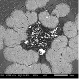
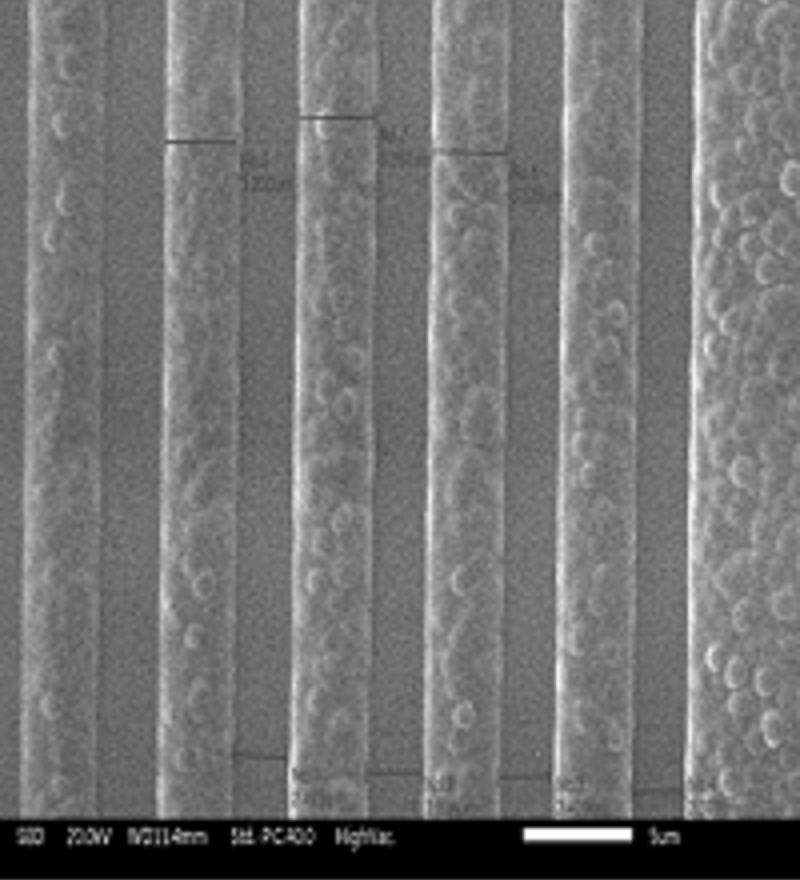
To complete this activity a sequential build up (SBU) way is adopted with an additive lithography process to realize any desired pattern with minimum possible feature size (<10 µm) on any substrate. A low cost insulating material, promising grafting solution and a UV Laser writing machine with optimized fabrication parameters are the highlights of this production method.. This activity is divided into three sub-activities which are as follows:
(a) Interconnects designing
(b) Microvia designing
(3) HDI designing
The reliability studies of the implementation are also the part of the project. This include use of different imaging methods (SEM, SAM, X-ray microscopy) with thermal cycling tests following the JEDEC standard JESD22-A104 with the temperature range of 0-100 oC with fall, rise and dwell time of 15 min resulting in 24 cycles per day. The inspection of the initial, intermediate and final condition of the implementations. Additionally, the performance monitoring using resistance method, DC and RF- based measurements ; thermal/humidity tests at 85°C temperature/85% relative humidity ("85/85") for up to a 2000-hour period.
The development of simulation models is also planned where these models either are compatible with the existing EDAs simulators or work in stand-alone as a calculator. The basis for these developments would be the statistics obtained from designing and testing. The purpose for the development is to reduce the efforts in the user training and also to estimate the performance of the wiring board before manufacturing
The usage of a metallization technology is proven in the highly competitive and cost sensitive high volume plating on plastics industry, e.g. metal on car/truck details, package metallization in perfume industry.
The enabling technology is a novel full additive metallization technology based on the Covalent Bounded Metallization process. The process exhibits excellent metal adhesion to polymers can produce metallization patterns based on UV lithography
Compact is aiming to provide an alternative, cheap and flexible fabrication methodology for HDI- PCB productions to local SME present in northern region.
The development procedure will be implemented at room temperature. Therefore, the PCBA industries will have cost-effective mass production with unlimited reproduction capabilities, and the most important is that the process would be highly controllable.
The waste management of the proposed method is simpler when compared with conventional PCB waste management. Because of use of fewer number of chemicals in small quantities are required in manufacturing process.
COMPACT is based on the Sequential Build-Up Technology thus, with appearance of new metallization materials or upgraded lithography, it will update itself easily.
Compact offers easy integration to the existing PCB production setup. The methodology will easily co-ordinate and synchronize with their current activities.
Compact aims create a feedback loop among academia, SME and technology experts. Compact listen to the all for their comments and remarks to analyze and implement.
The CBM process is today developed for plating on plastic in applications which have requirements for a highly robust adhesion of metal to polymers. CBM process to metallization of embedded die interconnects and the above given sub-part/components.
Acharya, S.; Chouhan, S.S.; Delsing, J. Fabrication Process for On-Board Geometries Using a Polymer Composite-Based Selective Metallization for Next-Generation Electronics Packaging. Processes 2021, 9, 1634. https://doi.org/10.3390/pr9091634
Acharya S., Chouhan S.S. and Delsing J., "An Additive Production approach for Microvias and Multilayered polymer substrate patterning of 2.5μm feature sizes," 2020 IEEE 70th Electronic Components and Technology Conference (ECTC), 2020, pp. 1304-1308, doi: 10.1109/ECTC32862.2020.00206.


To know more about the project and associated research activites please contact at compact.nord2019@gmail.com
Follow us on Facebook, Twitter and Linkedin at InterregNord Compact
Information about the EU program Interreg Nord is available at https://www.interregnord.com/.
To get in touch with Regional Council of Lapland at https://www.lapinliitto.fi
